
Capabilities - Skill sets for a new age

APS offers a variety of Scientific, Application, and Design Engineering services. Our professionals have been working together for over a decade on everything from advanced product design to basic proof of concept research and systems.
Let APS staff your short and long term needs with just the right skill for the job.
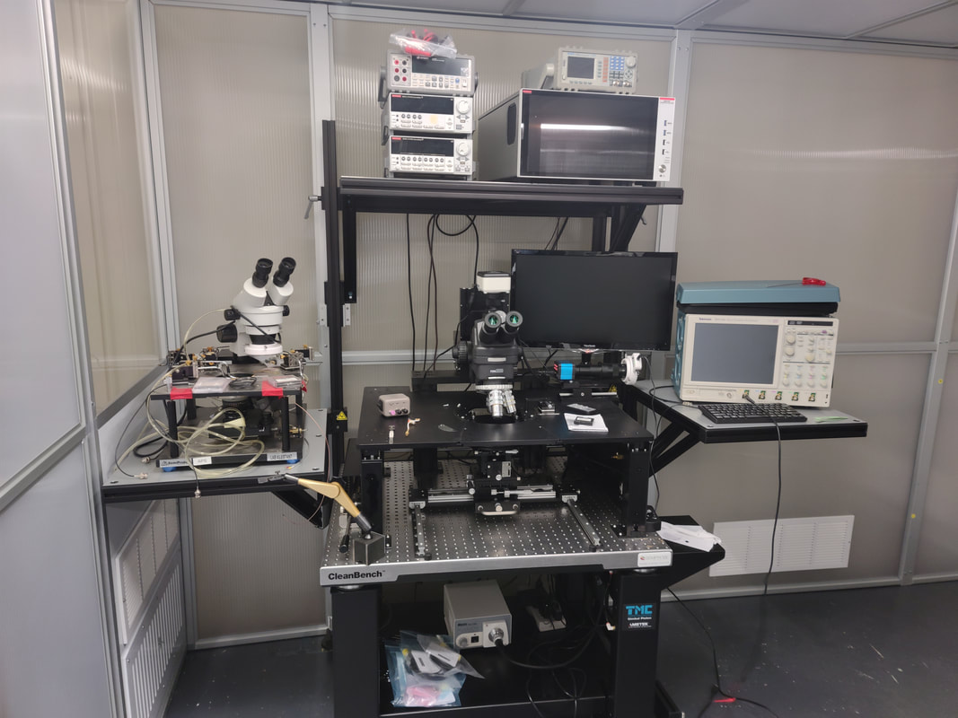
A variety of advanced instruments allows our team to provide detailed testing and analysis services.
Advanced packaging design, custom circuit design, embedded logic and control systems
Advanced packaging design, custom circuit design, embedded logic and control systems
Some of our unique capabilities include:
- Atomic Layer Deposition, ALD
- Metal and Dielectric sputtering
- High resolution direct write Lithography,
- 100nm e-beam on 100mm substrates
- 400nm on 200mm substrates (DLP Optical 385nm)
- 100nm e-beam on 100mm substrates
- High power short burst laser systems
- Product Design
- Optics Design and Testing
- Custom circuit design; multi-layered PCB and surface mount technologies
- Wafer probe testing
- Wafer probe testing
- ASIC circuit design Clewin and DW-2000 workshop
- Mechanical design and advanced machined part capability
- Fusion, FEA, Solid modeling
- Fusion, FEA, Solid modeling
- Applications development and support
- Field service and customer support
- Soldier personal protective gear (eye wear)
- Industrial controls and automation
- Reporting and production compliance